I’ve spent the last week learning about Fritzing to create printed circuit board art work. It’s a cool program with a quick learning curve. You might enjoy this quick video. It’s a great demonstration introduction. (Note: Fritzing is not limited to adduino)
I also spent a bit of time trying to produce a PCB board. After quite a bit of frustration I learned it’s pretty easy to do.
The numerous tutorials I found weren’t exaggerating. Turns out it was the laser printer I was using, an HP Color CP2025. Love that printer. But $50 bucks at Office Depot bought me a Samsung ML-1865W monochrome laser printer. Once I had this new printer I produced this board with my second try at applying the art work to the copper using the toner transfer method. Turned my frustration into excitement for using this technique for lot’s of electronics projects. It’s not much more time and effort than doing it on a perf board and it’s quite a bit more durable. You can send the circuit you create to a fabrication house for production too once you come up with that great idea for a new product.
After checking out the various tutorials in the Resources section below I highly recommend the Yahoo group: ‘Homebrew_PCBs’ Big win here was Staples item# 633215 Color laser paper. $12.49 / 300 =~ .042 cents per sheet. I also bought some 3M color transparency paper at Office Depot for the sticker shocking price of $35.49 / 100 =~ 35 cents a sheet. I haven’t tried the transparency subsequent to the laser printer purchase. For that price I can deal with the few shards of paper that stick to the artwork.
I’m assuming you’ve read one of the tutorials and are familiar with the terms used in the remainder of this post.
This is a nice little video from Instructables. Check the links in the Resources section of this post. Doesn’t hurt to read a couple different tutorials to drive the concepts home.
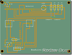 This is the PCB view in Fritzing of the board I created.
Here are a few pictures of my first circuit board using the toner transfer method.
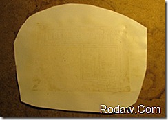 I’ve printed the artwork on the paper and laid it on the copper.
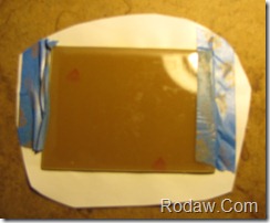 I taped it from behind. That way the tape doesn’t cause a high spot so it makes it easier to apply even pressure and heat. And you don’t gum up your artwork and iron with the adhesive from the tape.
 I set the iron half way between Wool and linen. I might try just a little cooler. Note in the first picture how the paper has wrinkled a bit. I heated it for less than three minutes. And moved the iron around a bit to be sure I had heat and pressure over all the art work.
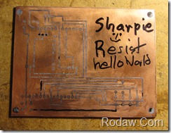 I had some bare copper so I tested a Sharpie and a special Etch resist pen from MG Chemicals obtained at Fry’s for like seven dollars. It even says sharpie on it! I don’t see any difference in the effectiveness between the generic Sharpie and the ‘etch resist pen’ Now we know. Save some bucks. Note that the S in the word Sharpie I traced over a couple times letting the first coat dry. The word Resist was done with the etch resist pen, I also doubled the application on the letter R. Looks like a single coating works.
I touched up the bottom trace a bit. You can see the line looks a bit jagged with the sharpie and is reflected in the copper trace below.
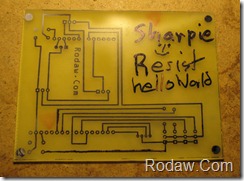 Out of the etch now, I used Ferric Chloride.
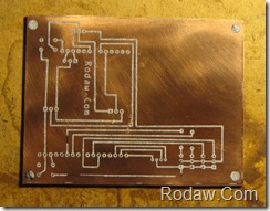
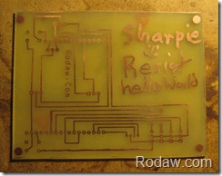 And here is the finished board after I used some lacquer thinner to remove the tonner and Sharpie resist. I’m pleased with these first results and can see that I’ll be able to produce more complex boards at home soon. It really is pretty easy. – Once I got the right laser printer. (
Note I’ve read many posts that say the Brother laser printers have to high a melting point for the toner transfer method to work at home.)
Resources:
http://fritzing.org/learning/tutorials/pcb-production-tutorials/diy-pcb-etching/
http://gilmore2.chem.northwestern.edu/projects/garbz2_prj.php
http://www.pocketscience.com.au/etching/etching.html
http://www.semis.demon.co.uk/PCB/PCB.html
http://pldaniels.com/flying/howtos/creating-printed-circuit-boards-part-I/
2 replies on “Journey to PCB”
http://www.pcbfx.com/main_site/pages/start_here/printer_info.html
GO here and read about the laser printers. Color lasers are a no go for toner transfer not enough plastic in the toner to do a transfer. I have done over 200 transfers using pulsars papers and films and a hot roll laminator and very few failures. I’ve used about every other type setup and this is the best by far to me.
Terry
[…] Boe-Bot from Arduino and Netduino. I’m building a PCB shield to support both platforms. Check out my effort to move from concept, prototype to PCB board. I learned about Fritzing and etched my own PCB at […]